Enabling the Transition from Research to Volume Production of Quantum Computing Chips
Particles exhibit an array of useful properties due to their quantum nature. Magnetism and the polarization of light are two examples of macro-scale manifestations of the quantum nature of matter and electromagnetic energy. Clearly, photons have useful quantum properties. And in fact, they are broadly useful for quantum computing. They can form the basis for some types of qubits, and even for other qubits they allow adiabatic (non-heat-generating) information interconnection into and out of the computer and between its elements. In addition, in implementations such as trapped-ion computing, photons are leveraged to immobilize and cool the qubits.
With technologies proven in several photonics applications and more to come, PI supports the further development of Quantum Photonics and thus promotes the transition from research to volume production.
Exploring Nitrogen-Vacancy Center Defects (NV)
The photonic emission of atomic-scale point defects in diamond crystals is of particular interest. For one example, when a carbon site instead contains a nitrogen occupant (a nitrogen-vacancy center defect) and is then illuminated with a stimulating laser, these defects can generate streams of photons of complete randomness, with no history or relationship between one emitted photon and the next. This is a valuable quality for quantum work. The NV centers can be manipulated in other ways too to alter their behavior in useful ways.
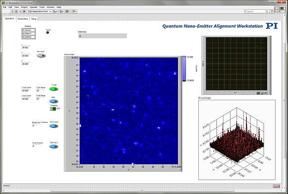
To locate and characterize these atomic-scale single-photon emitters, researchers at Purdue University and now the University of Illinois devised a clever workstation with PI’s participation. This workstation is based on an inverted microscope, a P-561 nanopositioning stage from PI is used as a carrier for the diamond sample. The stage is controlled by an E-712 controller from PI with photonic scan and alignment functionality integrated in the firmware. The sample is scanned with a fast, single frequency area scan that minimizes vibrations while an external photon counter detects the emitters. The controller's integrated data recorder records the information from the photon counter (presented as a voltage representing photon counts per millisecond) and stores it in a table along with the position of each data-point. The resulting fine map shows where NV centers are located. By clicking on an interesting emitter on the screen, it can be approached again and analyzed further. Another function in the firmware of the PI E 712 controller comes into play here: the gradient search. This enables tracking of the emitter to be analyzed. Changes in position, e.g. due to disturbances or temperature fluctuations, can be compensated.
The whole workstation is scriptable by an external program written in virtually any language, such as Python or MATLAB. This can repetitively "press the buttons" and read information from the workstation's responsive graphical user interface, allowing total automation very easily. The result has been an impressive set of published papers including details of the development of the brightest single-photon sources to that date using this technology.
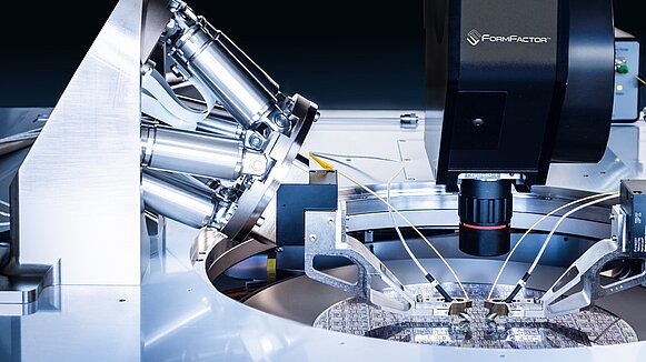
Wafer Probing
The combination of silicon photonics technologies and quantum technologies is very seductive. It can mean that the established infrastructure of semiconductor manufacturing could be leveraged for high-volume manufacturing of chips with quantum-technology elements.
This, of course, depends on exquisite construction and performance of the factory equipment. And it requires rigorous testing of designs from the earliest prototype chips to final production. In fact, the interval between those two phases of testing can be years. But, when a product reaches that stage, it means production is within sight!
The most important electrical and photonic testing begins at the wafer level. This is certainly useful during engineering and development and is absolutely critical for production economics once the design has advanced to volume manufacturing. After all, most of the cost of a packaged chip is in its packaging, so allowing a faulty chip to proceed through packaging is an expensive error.
Wafer probers are common, but wafer probers capable of high-throughput photonic testing are elite entrants in the field, available from just a handful of qualified manufacturers. Pioneering photonic wafer prober manufacturer FormFactor has optimized its fast photonic probers for testing of quantum computing chips.
The news that quantum-computing wafers were already undergoing wafer-level testing caught many industry observers by surprise. It means the path to volume manufacturing is clarifying... and short.